Technology
Technology news
Active contribution to the photonics community at SPIE Photonics West
SPIE Photonics West, held in San Francisco from January 27 through February 1, 2024, was a terrific opportunity for ams OSRAM to actively engage with customers and collaboration partners in the photonics community.
In-plane sensing in microLED displays
A new performance and manufacturing paradigm for optical sensing in consumer and automotive electronic devices.
ALIYOS™ LED-on-foil technology
Introducing the new ALIYOS™ technology from ams OSRAM: this innovative LED-on-foil technology enables unprecedented effects in automotive lighting, effects where the light comes almost out of nowhere.
Light-emitting diodes (LEDs)
Light-emitting diodes (LEDs) are semiconductor components which emit light when current flows through them in a forward direction. Electrons recombine with holes in the depletion zone releasing energy in the form of photons. The electrical characteristics of LEDs correspond to the electrical characteristics of normal diodes.
ams OSRAM’s comprehensive LED portfolio covers a vast array of diverse needs, applications and advanced technological solutions. Our technology offers highly efficient LED with improved color quality and durability.
Pixelated LED technology: pixelated light sources enable simultaneous visualization and illumination in a single component.
ams OSRAM chip-packaging technologies
Chip-packaging technologies developed by ams OSRAM help our state-of-the-art optical devices and sensor products to achieve extreme high precision, low noise performance and reduced system costs.
Advanced packaging technologies from ams OSRAM include:
-
Wafer-level optics, which enable the precise fabrication of lenses for miniature light sources and detectors
-
Through-silicon vias, which radically reduce the height of an optical IC package and eliminate the need for wire bonds
-
System-in-package (SiP) technology – ams OSRAM integrates complete sensor assemblies into a single SiP to save space and eliminate a board assembly process for customers
-
Stacked dual die – wherever reliability is a must, ams OSRAM offers fully redundant solutions with two of the same sensor dies in a single IC package.
Depth & 3D sensing
Structured light, passive/active stereovision, integrated Time of Flight, direct Time of Flight or intensity proximity? A wide range of optical sensing techniques exist to sense distance and capture 3D scenes, and all have different trade-offs. ams OSRAM enables designers to choose and implement the solution that matches their application best, through a comprehensive portfolio of illuminators, sensors and drivers.
Capacitive sensing
Capacitive sensing is a widely used technology in human presence detection, fluid-level sensing or hands on detection for autonomous driving. It works on the principle of capacitance: charge accumulates in the gap between two sheets of metal, or ‘electrodes’, when a voltage is applied to one electrode. The amount of charge which accumulates depends on a property, the ‘permittivity’, of the material between the electrodes.
At the heart of the capacitive sensor measurement system is a type of capacitive sensing technology called I/Q demodulation. This method measures the resistive as well as the capacitive element of a system’s impedance. The effect of this is that, unlike other methods for capacitive sensing, it works reliably even in difficult conditions, and is sensitive to small changes in resistance.
CMOS imaging
ams OSRAM continuously develops new technology to improve the performance of its CMOS image sensors. These technology improvements support both custom CMOS image sensor developments and standard, off-the-shelf CMOS image sensor products.
Position sensing technologies
Unique technology developed by ams OSRAM protects position sensors from interfering magnetic stray fields and reduces angle error so that – despite often harsh environments – they operate with accuracy and reliability.
Stray-field immunity: ams OSRAM position sensors feature a unique technology which protects them against interference from magnetic stray fields. The sensors overachieve ISO 11452-8, which specifies tests for the electromagnetic immunity of electronic components to magnetic fields for passenger cars and commercial vehicles regardless of the propulsion system.
Dynamic angle error compensation (DAEC™): DAEC™ is a revolutionary recent technology that yields almost zero output latency and ultra-fast refresh rates in high-speed motor control systems.
Coil design: the inductive position sensor technology is based on measuring the coupling between the coil (excitation and receiver coil) via rotating target. Due to its flexibility, easy adaption and low overall system costs, inductive position sensing acts as the perfect resolver replacement and can be used for on-axis as well off-axis applications.
PSI5 interface: PSI5 is a standard bus which enables communication between devices in an automotive system over a twisted-pair cable.
Spectral sensing
By shining light on or through objects and by looking at the reflected or transmitted spectrum, a sensor system can detect or classify what it is looking at.
Advantages of ams OSRAM spectral sensing technology:
- Interference filter technology for durability and spectral stability over time and temperature
- In-house filter manufacturing and testing capability
- In-house module design and manufacturing capability including
- Detectors
- Light source
- Light path
- Optics
VCSELs for flexibility and reliability
Vertical-cavity surface-emitting lasers (VCSELs) have various advantages over other types of lasers. These include:
-
surface emission, which offers design flexibility in addressable arrays
-
low temperature dependence of the lasing wavelength
-
superior reliability
-
a wafer-level manufacturing process
ams OSRAM VCSEL technology includes the epitaxial structure and chip design, epitaxial growth, front- and back-end processing, packaging and advanced testing and simulations. ams OSRAM VCSELs are rated for operation at ambient temperatures as high as 150°C.
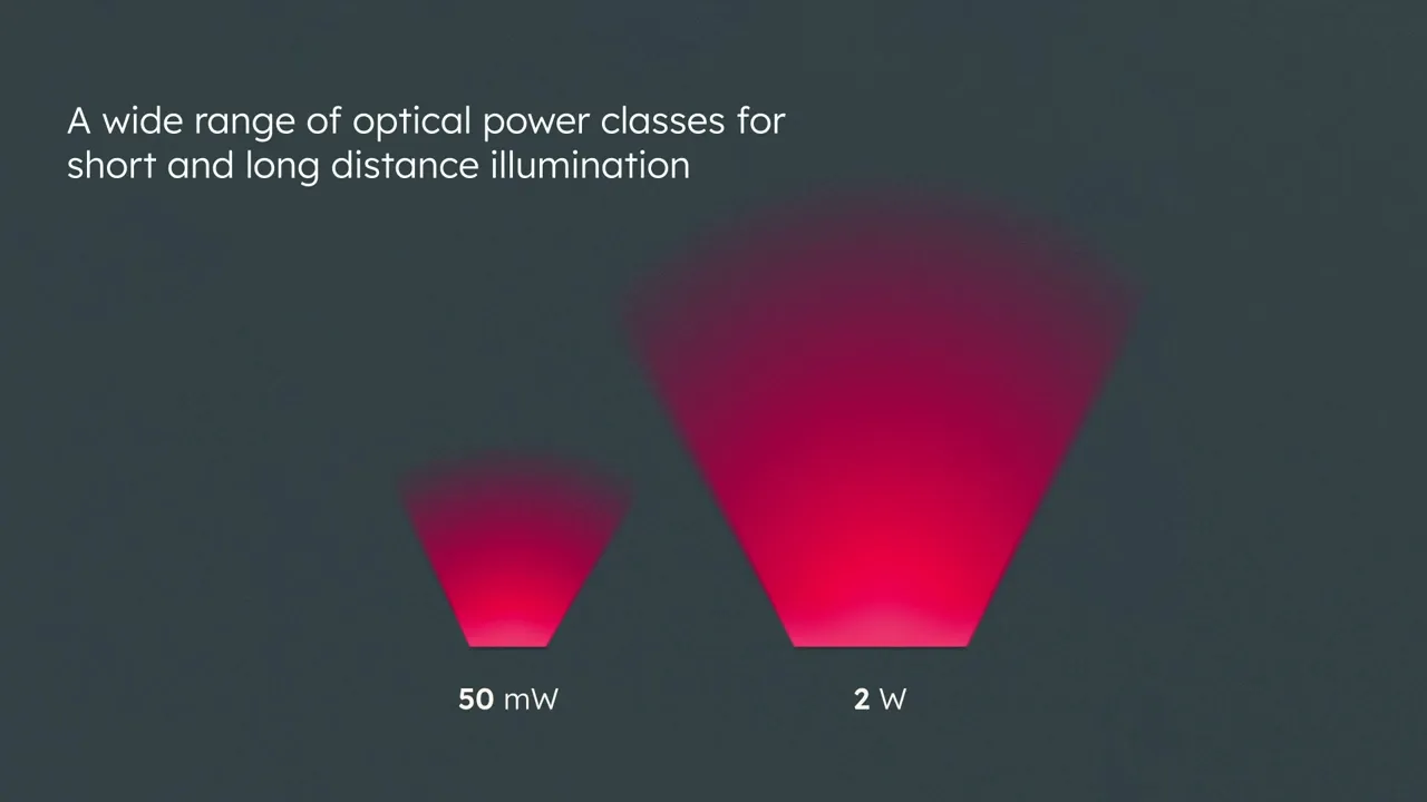
Infrared LEDs for invisible applications
Infrared illumination plays a significant role in the broad fields of industry, automotive and consumer applications: CCTV, biometric identification, driver monitoring, machine vision to name only a few.
With a long history in developing infrared LEDs, ams OSRAM is the industry leader in this technology, offering a range of products to match the varying requirements of each application area:
-
wall-plug efficiencies well above 50%, based on ams OSRAM’s thin-film technology
-
low operation voltage and extremely high-power ratings/low thermal resistance
-
wavelengths of 850nm and 940nm
-
various beam angles
-
Single- and dual junction (stack) chips
Continuously expanding and improving the IR LED portfolio, ams OSRAM is well-positioned to remain the market leader in infrared illumination.
> Discover more about IR illumination
Edge-emitting lasers (EEL)
ams OSRAM leads in visible and infrared edge-emitting lasers (EEL) technology for sensing, visualization and material processing.
Edge-emitting lasers use nanostack technology (e.g.: triple-junction: three light-emitting surfaces (pn-junction) stacked one on top of the other), which has the main advantage of delivering high power within a small area (small size), making it the technology of choice for long-range LiDAR, visualization, illumination and material processing.
Infrared laser diodes for sensing (LiDAR applications) with wavelength of 905nm have the highest efficiency on the market. The laser diodes can operate with extreme short pulses (down to 2nsec), while delivering outstanding power.
Visible InGaN laser diodes for laser projection and illumination have a great optical output power at high operating temperature range. Single-mode laser diodes can operate at a higher temperature range without active cooling and have excellent efficiency, which can extend long life.
High power performance with multi-mode laser diodes are the best fit for industry and automotive applications.
> Explore our laser competence
Micro-lens arrays (MLA)
Micro-lens arrays (MLA) operate as ultra-small projectors which have images integrated into the micro-optic lens, producing sharp images in brilliant color. Micro-lenses offer a long focal depth, which means that an array can project a focused image on to a parallel, slanted or curved surface.
Micro-lens arrays may be configured to provide a bright output in an extremely low-profile form factor. In conventional projector technology, the higher the brightness required, the larger the projector. By contrast, micro-lens arrays can be arranged next to each other so that their images overlap to create a brighter picture, while the thickness of the projector, typically 3mm, remains the same.
Micro-lens array technology from ams OSRAM used in the automotive sector and in various non-automotive applications.